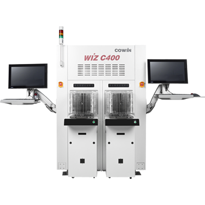
Wafer/wafer Bump Inspection
& Laser Cleaner

& Laser Cleaner
A technology for producing equipment that detects
surface defects on Wafer/Wafer Bumps during the semiconductor
manufacturing process, and cleanses Foreign Material using a laser.
Semiconductor
A method for making equipment that spots surface flaws on
Wafers in semiconductor production processes and removes foreign material defects.
Wafer Bump Inspection
WLP (Wafer Level Package) Process adaptation
Solder Bump, Gold Bump, Cu Pilar Precision
measurement
LED/LASER Lighting implementation
2D/3D Consistent inspection
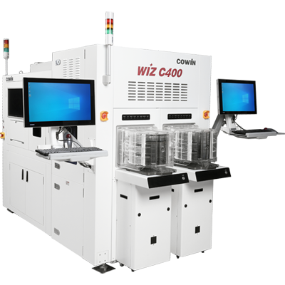
Wafer LASER Cleaning
Linking inspection equipment data
Laser cleaning of Foreign Material
without harming patterns