반도체 제조 공정에서 사용되는 중요한 기술로서,
반도체 Wafer 표면에 발생하는 다양한 이물질 또는
오염물질을 제거하는 기술입니다.


Mold Residue Cleaner
다양한 이물질 및 오염물질을 제거하여 깨끗한 표면을 만들어 줌으로써,
반도체 소자의 정확성 및 신뢰성을 보장하며, 제품의 품질을 높이는 역할을 수행합니다.
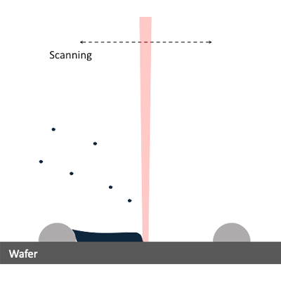
Laser Removing
Target: Metallic Residue, Foreign Matter, Organic Matter
Residue
Principle: Physical/Thermal Processing of Focused Laser
All-Surface Scan Processing to Minimize Wafer/Bump
Damage
Scan Processing of Recognition of Residue/Foreign
Matter Defect Areas
Point Matching and Processing of Foreign Matters
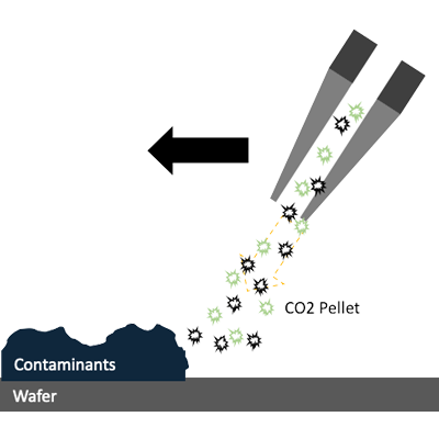
Residue Cleaning
Target: Organic Matter Residue, Byproduct of Laser
Processing
Principle : Physical Collision, Thermal Collision
Shrinkage/Expansion
Physical Collision and Breakaway between Particles and Compressed Air
Rapid Cooling(-70 ~ 80 ℃) for Shrinking Deformation
800x Expansion of CO2 Particle to Destruct
Contaminants
Vaporize Directly at Room Temperature and
No Secondary Contamination
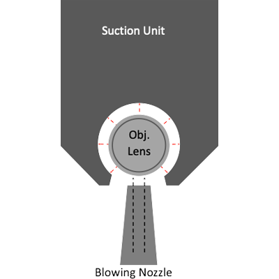
Blowing & Suction
Target: Byproduct of Processing, Floating Matter, Gas
Principle : Floating Matter/Gas Flow
Flow Occurrence of Anisotropic Blowing Floating Matter
Isotropic Suction for Preventing Secondary
Contamination